DKN Research Co-Develops Ultra Thin Copper-Free Flexible Circuits As Small As 0.2 Micron Thick with Micro via Holes for Scientific and Medical Devices

August 6th 2012
News Release from DKN Research, Haverhill, Massachusetts, U.S.A.
“DKN Research Co-Develops Ultra Thin Copper-Free Flexible Circuits As Small As 0.2 Micron Thick with Micro via Holes for Scientific and Medical Devices”
DKN Research, a leading engineering firm specializing in microelectronics and packaging technology, now carries ultra thin copper-free flexible circuits with reliable via holes. The Haverhill Massachusetts based firm developed a series of processing technologies to generate thin nickel traces on both sides of thin polyimide film specifically targeting those scientific and medical applications that require the elimination of copper metals from electronic devices. It also provides a wider range of design flexibilities for packaging and termination in special electronic circuits. DKN Research continually develops a wide range of packaging technologies for flexible & printable electronics.
Virtually all printed circuit boards use metal copper for their conductive material because of its high conductivity and reasonable cost. Unfortunately, several electronic devices designed for scientific and medical equipment can not have metallic copper in the circuit because of its physical properties and chemical instability. There are a few metal foils such as aluminum and stainless steel that can serve as the conductor material, but they cannot be thinner than 10 microns. Another problem with these metals and alloys is the difficulty in via hole formation for double side and multilayer circuits.
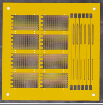
DKN Research partnered with Pyramid Technical Consultants, Inc, a specialty electronic module manufacturer from Lexington Massachusetts, and co-developed many kinds of copper-free flexible circuits combining various technologies such as sputtering, plating, chemical etching and laser abrasion & drilling. The team recently announced the success in establishing a new manufacturing process to generate ultra thin nickel traces down to 0.2 microns thick on both sides of thin polyimide film with small via hole connections down to 80 micron diameters. Special polyimide etching process and laser drilling process were employed to generate tiny holes on thin polyimide films. A new electroless nickel plating process was developed to make uniform conductive layers on the surface and inside the polyimide film holes. A set of chemical etching process and laser abrasion process were furnished to make fine traces down to 50 microns line and space. The small via holes formed by this new process are very reliable, and remained intact during the heat cycle and flexing endurance tests.
DKN Research and Pyramid Technical Consultants agreed to disclose all the information pertaining to their new technology and share the unique process with other researchers and engineers. This unique circuit manufacturing can work with other circuit processing technologies such as copper etching and screen-printing to enhance the capabilities of any special application. Technical reports are available by requests, and the two engineering teams can support both prototype trials and volume productions.
Click on the link below to view a short clip about their products and services:
DKN Research is a worldwide engineering leader for microelectronics and packaging, specializing in printable & flexible electronics. DKN Research has developed a broad range of leading edge technologies from materials to final devices based on customers’ requirements. They are capable to manage many kinds of materials and manufacturing processes to build and create new devices based on customer needs.
DKN Research provides a broad range of engineering and consulting services not only for the manufacturing community but also the R&D and quality assurance professionals. DKN Research welcomes all inquiries to assist in creating your own circuit devices using its broad range of processing technologies.
Address:
DKN Research LLC,
62 Adams St., Haverhill, Massachusetts 01830-6862 U.S.A.
Phone: 1-978-372-2345 (General)
1-978-436-1417 (Customer Service)
For more detailed information, please contact us at following addresses:
Technical: Dominique Numakura, dnumakura@dknresearch.com
Business: John Rufiange, JohnRufiange@dknresearch.com
General (in the U.S.): 1-978-372-2345
Pyramid Technical Consultants is an industry leader for sensing and controlling systems. Pyramid designs and manufactures instrument control systems for medical and semiconductor equipment as well as physics research and biological research markets. The systems typically involve electronics hardware, embedded real-time software, and host system software drivers and applications. The Company specializes in low-current measurement and detector system readout.
Address:
Pyramid Technical Consultants, Inc.
1050 Waltham Street, Suite 200
Lexington, MA 02421, USA
Phone: 1-781-402-1700 (General)
URL: www.ptcusa.com
Attached: Test coupon of the ultra thin nickel circuits with micro via holes
Monday, August 6, 2012