My Blog

Transparent Materials and Flexible Circuits
Transparent Flex Circuits
DKN Research has been developing transparent & heat resistant circuits. There are several choices for both of materials and manufacturing processes to build transparent circuits, therefore, the circuit designers can choose the best construction for the goal.
1.Substrate materials
Currently, there are three vendors for transparent polyimide films.
Electrical properties are equivalent as the traditional polyimide films. They are all heat resistant against soldering or wire bonding process. There are several differences with physical properties and surface properties.
Standard thickness: 25 micron thick
**Thicker and thinner films will be available by requests.
Transparent PEEK film is under evaluation. It could have higher physical properties and stable chemical properties compared to the traditional polyimide films with wider thickness ranges.
2. Conductors
*ITO sputtered (Transparent, <150 ohm sq.)
*PEDOT ink screen-printable (Transparent, <150 ohm sq.)
*Silver ink screen-printable (<20 ohm sq.)
*Graphite ink screen-printable (>200 ohm sq.)
*Ag nanowire ink screen-printable (Transparent, <80 ohm sq.)
*Thin Ni/Cu/Au plated down to 0.2 micron thick (<10 ohm sq.)
*Rolled annealed copper foils laminated with glue
The transparency could be 20% lower than bare PI films.
Thickness: 9, 12, 18 and 35 micron thick
3. Laminates
Several combinations with transparent polyimide films are available for chemical etching and laser abrasion processes.
*ITO coated films
*Metal plated, double sided
Electroless Nickel: < 0.1 micron thick
Electro-plated copper: 0.1 to 5 micron thick
Electro-plated gold: 0.05 to 0.5 micron thick
*Metal foil laminated with glue
Rolled annealed copper foils laminated:
9, 12 and 18 micron thick
4. Cover layers
There are two types of transparent cover layers.
*Transparent films with glue
Total thickness: 50 micron
It reduces transparency 40%.
*Transparent epoxy ink
Thickness: down to 15 micron
It reduces transparency 20%.
5. Circuit constructions
*Single side circuits with or without cover layer
Conductors, transparent:
ITO,
PEDOT: Line width: <200 micron wide
Ag nano-wire: Line width: <100 micron wide
Thin copper grid etched:
Line width: <500 micron wide
Conductors, non-transparent:
Thin copper plated:
Line width: <50 micron wide
Copper foil laminated:
Line width: <70 micron wide
Silver ink screen-printed
Line width: <80 micron wide
Graphite ink screen-printed:
Line width: <200 micron wide
Gold plating is available on the conductor traces.
(Electroless and electro plating)
*Double side with via or without cover layers
Conductors: Same as single side circuits
Via holes: Laser drilled down to 70 microns
NC drilled down to 150 microns
Nickel/Copper plated
Silver ink filled
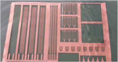
Photo: Transparent flex Circuit with Copper Traces
Wednesday, August 24, 2016
